Physical Vapor Deposition (PVD) vs Chemical Vapor Deposition (CVD)
@PhysicsMaterialsScienceandNano
Physical Vapor Deposition (PVD) and Chemical Vapor Deposition (CVD) are both thin film deposition techniques used extensively in various industries including semiconductor manufacturing, optics, and coatings. Here’s a comparison between the two:
Physical Vapor Deposition (PVD):
1. **Process**: PVD involves the physical transfer of material (typically through evaporation or sputtering) from a solid source to the substrate surface.
2. **Mechanism**: The material is evaporated or sputtered off a target source (solid metal, ceramic, etc.) in a vacuum chamber, and then condensed onto the substrate, forming a thin film.
3. **Energy Source**: PVD processes often rely on physical energy sources like thermal energy (for evaporation) or plasma (for sputtering).
4. **Advantages**:
Allows for precise control over film thickness.
Can deposit a wide range of materials, including metals and ceramics.
Good adhesion and density of films.
5. **Disadvantages**:
Limited to materials that can be evaporated or sputtered.
Limited by line-of-sight deposition, which can result in uneven coating thickness on complex geometries.
Chemical Vapor Deposition (CVD):
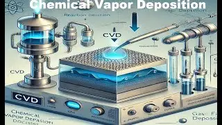
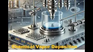
1. **Process**: CVD involves the chemical reaction of gases (precursors) on the substrate surface to form a thin film.
2. **Mechanism**: Precursor gases are introduced into a chamber where they react and deposit onto the substrate surface as a solid thin film.
3. **Energy Source**: Typically, CVD processes require thermal energy to initiate and sustain chemical reactions (although some variants like Plasma Enhanced CVD use plasma).
4. **Advantages**:
Can coat complex shapes and surfaces uniformly.
Allows for a wide range of materials, including semiconductors, metals, and ceramics.
Can produce very high purity films.
5. **Disadvantages**:
Deposition rates can be slower compared to PVD.
More complex setup and control due to the involvement of chemical reactions.
Key Differences:
**Mechanism**: PVD is a physical process (evaporation or sputtering), whereas CVD is a chemical process involving gas phase reactions.
**Material Compatibility**: PVD is typically limited to materials that can be evaporated or sputtered, while CVD can deposit a wider range of materials including compounds and alloys.
**Uniformity**: CVD generally offers better uniformity over complex geometries compared to PVD.
**Control**: PVD offers better control over film thickness, while CVD allows for precise control over chemical composition.
In summary, the choice between PVD and CVD depends on the specific requirements of the thin film application, including material composition, deposition rate, uniformity, and the complexity of the substrate geometry. Both techniques have their strengths and are chosen accordingly in different industrial and research applications.
*CVD:*
#ChemicalVaporDeposition
#ThinFilmTechnology
#GasPhaseDeposition
#MaterialSynthesis
#UniformCoatings
#ChemicalReactions
#SemiconductorManufacturing
#HighPurityFilms
#PrecursorGases
#PlasmaEnhancedCVD
*PVD:*
#PhysicalVaporDeposition
#ThinFilmDeposition
#EvaporationTechnique
#SputteringProcess
#VacuumDeposition
#MetalCoatings
#CeramicCoatings
#ThinFilmMaterials
#TargetMaterial
#ThicknessControl
chemical vapor deposition,
chemical vapor deposition (cvd) process,
chemical vapor deposition process,
chemical vapor deposition semiconductor,
chemical vapor deposition (cvd),
chemical vapor deposition carbon nanotubes,
chemical vapor deposition method,
chemical vapor deposition graphene,
chemical vapor deposition machine,
chemical vapor deposition diy,
chemical vapor deposition animation,
chemical vapour deposition and sputtering,
chemical vapour deposition applied physics,
chemical vapour deposition process animation,
plasma assisted chemical vapor deposition,
plasma assisted chemical vapor deposition pecvd,
chemical vapour deposition btech 1st year,
chemical vapour deposition carbon nanotubes,
chemical vapor deposition (cvd) process tamil,
cvd chemical vapor deposition,
cvd chemical vapor deposition in tamil,
chemical vapour deposition diamond,
diy chemical vapor deposition,
diamond chemical vapor deposition,
chemical vapour deposition engineering physics,
chemical vapour deposition engineering physics in telugu,
chemical vapour deposition explanation in telugu,
chemical vapour deposition explain in tamil,
explain chemical vapor deposition process,
plasma enhanced chemical vapor deposition