How To Test a PCBA (Printed Circuit Board Assembly)
Using IPC/JEDEC-9704 & 9702 Standards for Strain Gage Testing of Any Printed Wiring Boards.
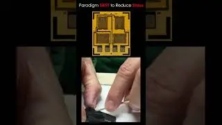
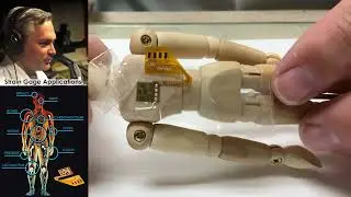
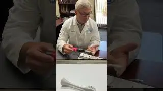
In this iNotes Video , Mike talks about cracks in the PCBs and shows how Micro-Measurements strain gage sensors are used when testing components, sub-assemblies, printed circuit boards, Ball Grid Array (BGA) surface mount packaging and finished products.
Who should use foil strain gage sensors: Test-fixture vendors, Component suppliers, Contract manufacturers (EMS), PCB assemblers.
Main problems: PCB failure due of over-flexure during various assembly and test processes, minor cracks and last but not least field returns.
The demand for reliable, durable and compact electronic devices is all around us. Consumer electronics, industrial, automotive, aerospace and medical device manufactures want it, “lighter, more compact, more durable, more powerful” and, oh by the way, all at a lower price. This demands that the product is designed, tested and manufactured to exacting standards to meet the expectations of an ever more demanding marketplace. These requirements have been further complicated by the elimination of leaded solder to be RoHS compliant. Lead-free solder is much more brittle and is susceptible to brittle fracture when exposed to excessive strain.
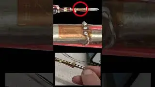
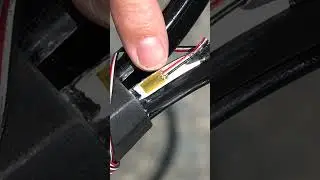
Cracks in the PCBs — brittle fractures in solder and even across components, particularly around BGAs — can be induced by in-circuit test fixtures and during assembly, burn-in and testing, system integration, and packaging and shipping. Strain measurements should be made after all design iterations of the PCB, including changes to on-board components, which may alter thermal stress loading. This is especially useful when introducing new solder materials and processes, which may have a different stiffness and introduce a different soldering thermal profile. The miniaturization of consumer electronics — and consequent increase in component density — results in larger thermal stresses, new requirements for surviving repeated loading, and a greater need for impact stress survival. Meeting these specifications requires accurate knowledge of strains in the PCB and on-board components. Strain gage measurement is the quickest, most accurate, and most cost-effective method for identifying strains on a PCB, and can be used in developing loading fixtures and test plans to optimize the testing phase.
IPC/JEDEC Standards IPC/JEDEC 9704 - Printed Wiring Board Strain Gage Test Guideline. IPC/JEDEC 9702 - Monotonic Bend Characterization of Board-Level Interconnects
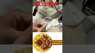
The solution is miniature-scale strain gage (gauge) sensors designed to meet the growing demand for precise, stable, and reliable stress analysis of PCBs, even in harsh environments
Strain Gauge Sensor Measurements on PCBs with Over 100 Years of Combined Experience (Webinar): https://www.strainblog.com/media/stra...
Micro-Measurements Announces Global Market Introduction of Miniature Planar Rosette Strain Gage Pattern for PCB Testing: http://www.vishaypg.com/micro-measure...
Training Programs and Schedules: http://www.vishaypg.com/micro-measure...
StrainTalks™ seminar: https://straintalks.com/
StrainBond™? https://strainbond.com/
StrainBlog: https://www.strainblog.com/